
NexXora develops hardware systems from embedded devices to more complex electronics, covering PCB layout and broader hardware development. The engineering scope connects functional requirements to a practical board design, with reliability, space, power and the eventual manufacturing process considered together.
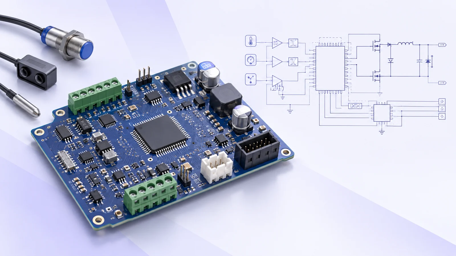
Start with the required interfaces, sensors, processing, power inputs and physical limits. The work package can include a block diagram, component selection and design trade-offs before detailed schematic capture.
Explore EDA services, high-speed digital and analog design, RF PCB design, signal-integrity and power-integrity work, and miniature PCB layouts. Each specialist page explains the engineering problem and the expected project inputs.
Application examples include industrial data-acquisition boards, IoT sensor nodes, controller interfaces, wearable electronics and power-supply control boards. Requirements such as connector placement, mounting points and access for testing should be considered with the mechanical design.
A release package includes schematics, bill of materials, PCB layout, manufacturing outputs and assembly information. Prototype bring-up and validation should be scoped explicitly so a manufactured board can be compared with its design requirements.
Share the product requirements, operating conditions, power limits, intended interfaces, mechanical envelope and expected volumes. Identify any parts that must be retained and any existing problems, such as noise, heat, unavailable components or a board that needs to shrink.
An IoT sensor board may combine power conditioning, sensor acquisition, processing and wireless communication in one enclosure. An industrial controller may need field connectors, protected inputs and a manufacturing test interface. Define these functions before choosing the component architecture.
A useful prototype review includes board startup, rail behaviour, peripheral access and mechanical fit. Identify the test points and measurements needed to investigate faults. Keep component substitutions and layout changes under revision control so the next manufactured board can be compared with the design that was evaluated.
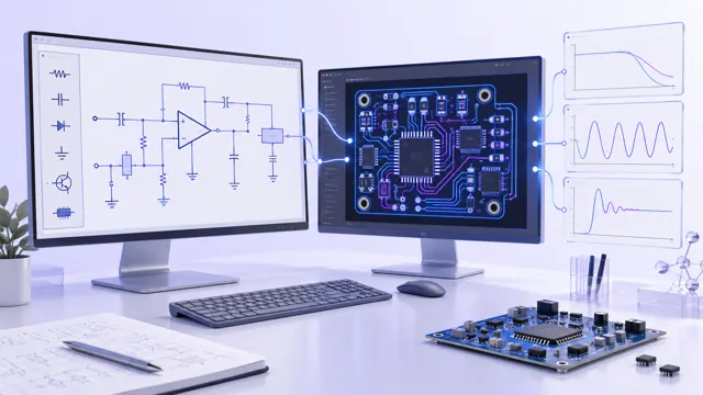
Turn electronic requirements into schematics, simulations and PCB design information that can be reviewed and manufactured.
Electronic Design Automation Services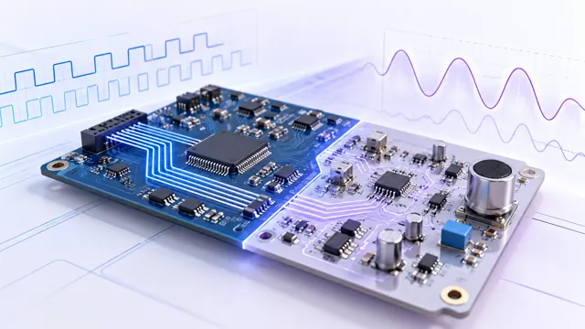
Design fast digital interfaces and sensitive analog circuits with layout constraints tied to signal quality and system requirements.
High-Speed Digital and Analog Design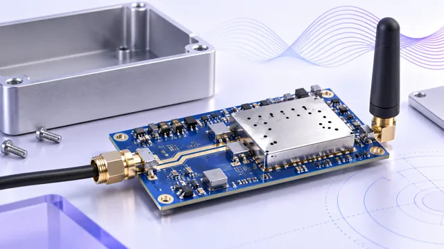
RF board layout, simulation and prototype support for wireless devices and high-frequency electronic assemblies.
RF PCB DesignMultilayer PCB design focused on clean signal paths, reliable return paths and controlled power delivery.
Signal Integrity and Power Integrity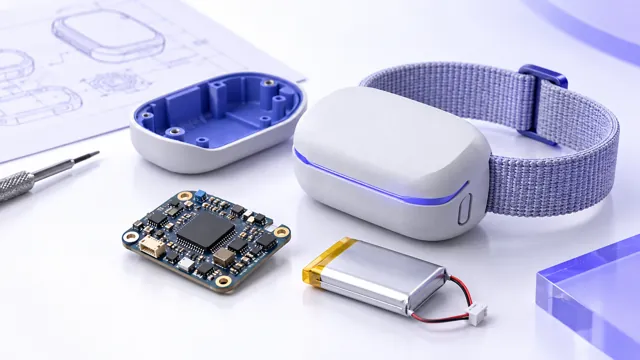
Compact, high-density electronic board design for wearables, sensor nodes and space-constrained products.
Miniature PCB Design